
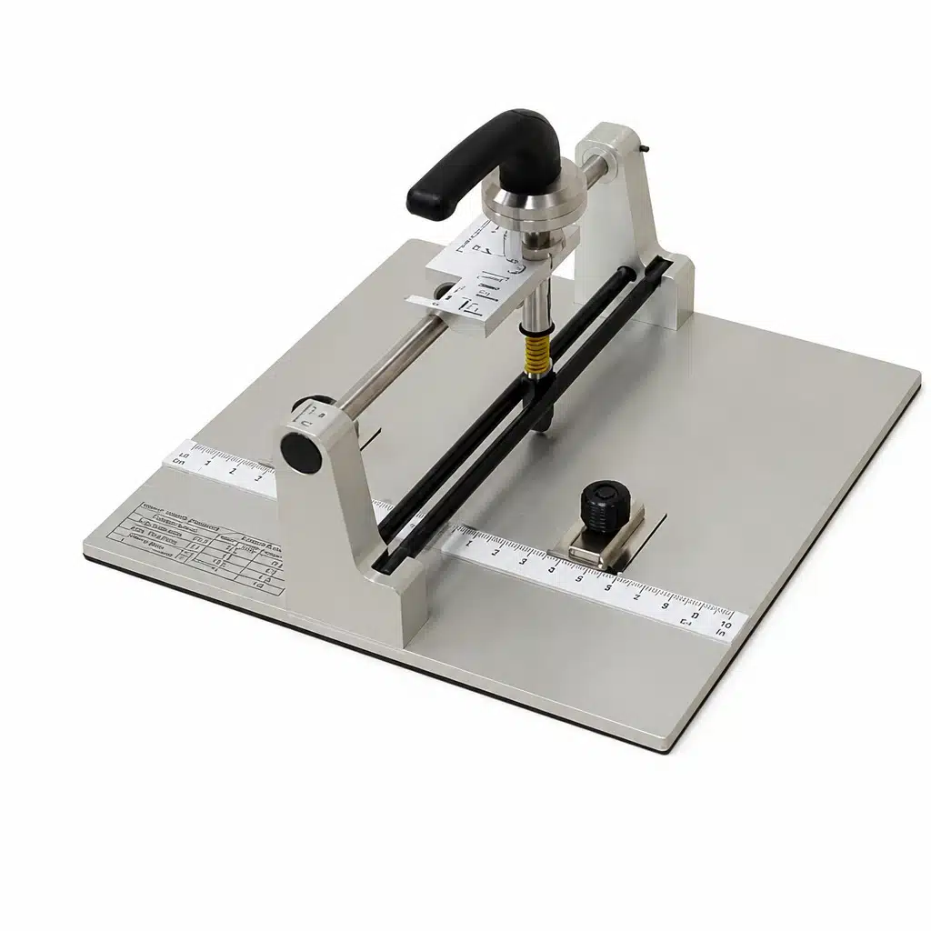
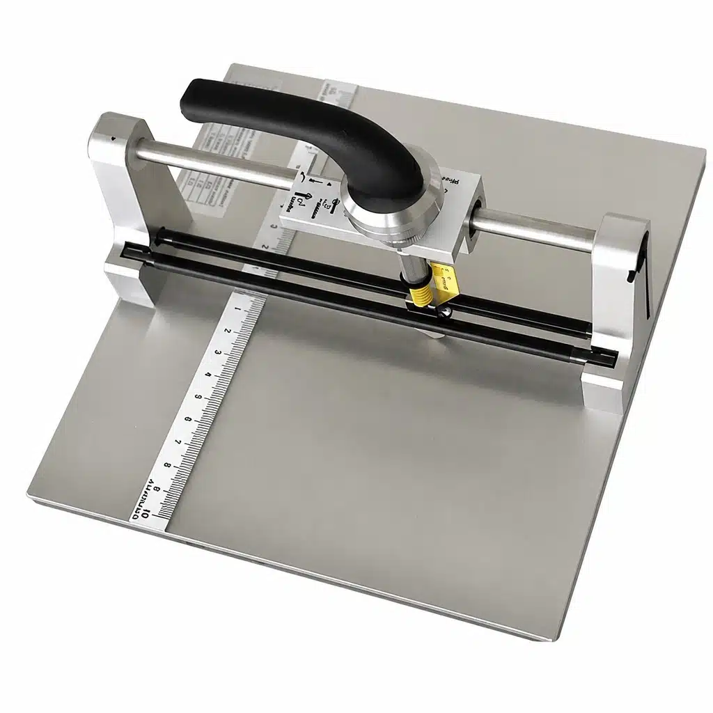
SYJ-DS100-LD Precision Manual Diamond Wafer Scriber for Single Crystal Wafers
The SYJ-DS100-LD is engineered for the accurate scribing of thin single crystal wafers such as Silicon, Sapphire, Germanium, Lithium Niobate (LiNbO3), and Lithium Tantalate (LiTaO3). It addresses the need for controlled substrate scoring prior to splitting, essential in semiconductor and crystal processing laboratories.
This manual scriber operates by applying an adjustable spring-loaded pressure to a diamond tip, allowing precise control over the cutting force. The device accommodates wafer sizes ranging from 100 x 100 mm (4″) to 300 x 300 mm (12″), with a maximum substrate thickness of 1 mm. The adjustable pressure ensures minimal damage while achieving effective scribing on delicate single crystal materials.
Wichtigste Merkmale
- Diamond scriber designed specifically for thin single crystal substrates including Si, Sapphire, Ge, LiNbO3, and LiTaO3.
- Spring-loaded mechanism allows fine adjustment of cutting pressure to suit material and thickness.
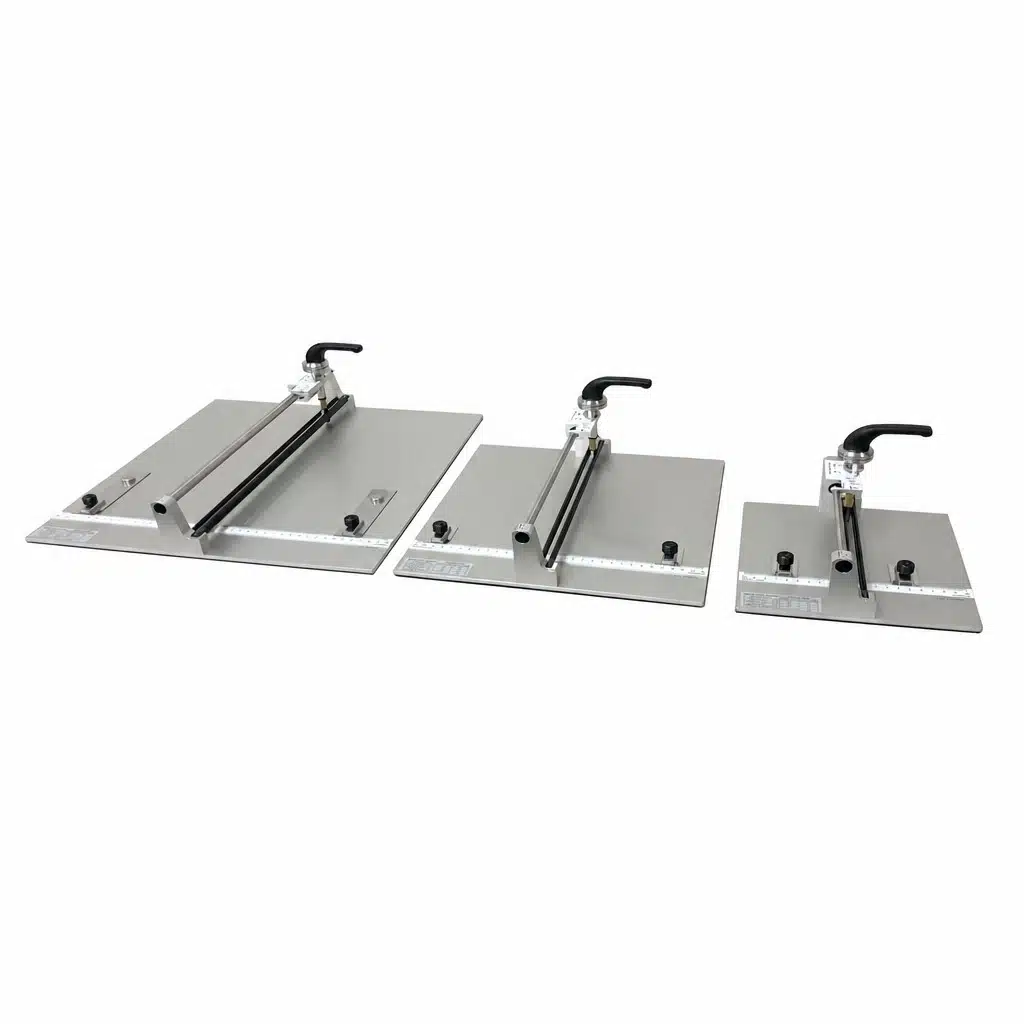
- Supports wafer sizes of 100×100 mm, 200×200 mm, and 300×300 mm (4″, 8″, and 12″ respectively).
- Maximum cutting thickness up to 1 mm for single crystal substrates.
- Includes one diamond cutting knife (13 mm x 26 mm x 5 mm) with 0.65 mm thickness cutting wheel.
- Made in Japan, ensuring high manufacturing quality and precision.
- Simple diamond scriber replacement procedure with included hex wrench.
Technische Daten
| Parameter | Spezifikation |
|---|---|
| Supported Wafer Sizes | 100 x 100 mm (4″), 200 x 200 mm (8″), 300 x 300 mm (12″) |
| Maximum Cutting Thickness | 1 mm |
| Cutting Wheel Thickness | 0.65 mm |
| Diamond Knife Dimensions | 13 mm (L) x 26 mm (W) x 5 mm (H) |
| Pressure Adjustment | Spring-loaded adjustable pressure dial |
| Material Compatibility | Silicon, Sapphire, Ge, LiNbO3, LiTaO3 |
| Origin | Japan |
| Stromversorgung | None (manual operation) |
Typische Anwendungsbereiche
This scriber is ideal for laboratories and production environments requiring precise scoring of thin single crystal wafers prior to cleaving or dicing. It is commonly used in semiconductor wafer preparation, optical crystal processing, and research involving fragile substrate materials.
Hinweise zur Konfiguration und zum Betrieb
The device includes one diamond cutting knife and necessary tools for replacement. Users should adjust the diamond scriber height and spring pressure according to substrate thickness and material hardness. After use, it is recommended to reset the spring pressure dial to zero to prevent spring degradation. Periodic lubrication of the guide rod is advised for smooth operation. The minimum substrate size should be at least twice the thickness, generally no smaller than 5 mm x 5 mm. Replace the diamond scriber promptly when it becomes dull to maintain cutting quality.
Maße & Versand
| Product dimensions | SYJ-DS100: 210 mm (L) x 210 mm (W) x 140 mm (H); SYJ-DS200: 310 mm (L) x 310 mm (W) x 140 mm (H); SYJ-DS300: 410 mm (L) x 410 mm (W) x 140 mm (H) |
|---|


